


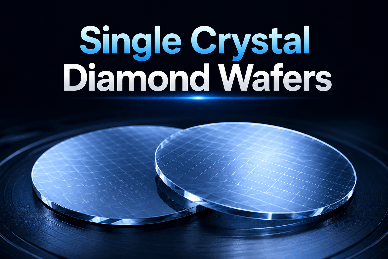
As industries continue to push the boundaries of innovation, the demand for advanced materials capable of delivering superior performance has never been greater. Modern technologies such as artificial intelligence (AI), semiconductor manufacturing, quantum computing, aerospace systems, medical devices, and high-power electronics require materials that can withstand extreme operating conditions while maintaining exceptional efficiency and reliability. Among the most promising materials meeting these demands are Single Crystal Diamond Wafers.
Renowned for their outstanding thermal conductivity, mechanical strength, optical transparency, and electrical insulation, Single Crystal Diamond Wafers are becoming an essential component in the development of next-generation technologies. Their exceptional material properties make them a preferred choice for industries where precision, durability, and thermal performance are critical.
What Are Single Crystal Diamond Wafers?
Single Crystal Diamond Wafers are high-purity synthetic diamond substrates grown with a continuous crystal lattice structure, meaning the entire wafer consists of a single, uninterrupted crystal. Unlike polycrystalline diamond materials, which contain multiple crystal grains and grain boundaries, single crystal diamonds offer superior structural uniformity and significantly enhanced physical properties.
These wafers are typically manufactured using advanced technologies such as Microwave Plasma Chemical Vapor Deposition (MPCVD) or High Pressure High Temperature (HPHT) processes. These techniques enable precise control over crystal growth, allowing manufacturers to produce diamond wafers with exceptional purity, consistency, and customized specifications.
The result is a premium material that delivers outstanding performance in demanding industrial and scientific applications.
Exceptional Thermal Conductivity
One of the defining characteristics of Single Crystal Diamond Wafers is their extraordinary thermal conductivity. Diamond is widely recognized as the best natural conductor of heat, outperforming traditional materials such as copper, aluminum, silicon, and ceramic substrates.
This remarkable property allows Single Crystal Diamond Wafers to transfer heat away from high-power electronic components with exceptional efficiency.
The benefits include:
- Faster heat dissipation
- Reduced thermal hotspots
- Stable operating temperatures
- Improved device reliability
- Enhanced system performance
As modern electronics become increasingly compact and powerful, efficient thermal management is essential for maintaining long-term performance.
Superior Mechanical Strength
Diamond is the hardest known natural material, making Single Crystal Diamond Wafers exceptionally durable and resistant to wear.
Their outstanding mechanical properties provide:
- High scratch resistance
- Excellent wear resistance
- Long operational lifespan
- Structural stability under extreme conditions
These characteristics make them particularly valuable in demanding environments such as aerospace systems, industrial manufacturing, and defense applications.
Excellent Optical Properties
Another major advantage of Single Crystal Diamond Wafers is their remarkable optical performance.
Diamond exhibits excellent transparency across a broad range of wavelengths, including ultraviolet (UV), visible, and infrared (IR) light.
This makes these wafers ideal for:
- Laser optics
- Infrared windows
- High-power laser systems
- Optical sensors
- Photonic devices
Their combination of optical clarity and thermal stability enables reliable operation in high-energy optical applications.
Outstanding Electrical Insulation
Unlike many metals used for heat dissipation, diamond is an excellent electrical insulator.
This unique combination of:
- High thermal conductivity
- Excellent electrical insulation
- Chemical stability
makes Single Crystal Diamond Wafers highly suitable for advanced semiconductor packaging, power electronics, and radio-frequency (RF) devices where electrical isolation is essential.
Applications Across Multiple Industries
Semiconductor Industry
The semiconductor industry is one of the largest adopters of Single Crystal Diamond Wafers.
As processors become faster and more powerful, heat generation continues to increase. Diamond wafers are used to improve thermal management in:
- Power semiconductors
- RF amplifiers
- Laser diodes
- High-frequency devices
- AI processors
By efficiently dissipating heat, they help improve device performance, reliability, and lifespan.
Quantum Computing
Quantum computing requires materials with exceptional purity and crystal perfection.
Single Crystal Diamond Wafers are increasingly used in:
- Quantum processors
- Quantum sensors
- Nitrogen-vacancy (NV) center devices
- Quantum communication technologies
Their stable crystal structure enables researchers to manipulate quantum states with remarkable precision, making them an important material for future quantum technologies.
Aerospace and Defense
The aerospace and defense sectors demand materials capable of operating reliably under extreme temperatures, pressure, and radiation.
Applications include:
- Satellite systems
- Radar technology
- Space electronics
- Defense communication equipment
The durability and thermal stability of Single Crystal Diamond Wafers make them highly suitable for these mission-critical environments.
Medical Technology
Medical devices increasingly rely on precision optics and advanced electronic systems.
Single Crystal Diamond Wafers are used in:
- Medical laser systems
- Imaging equipment
- Diagnostic instruments
- Surgical technologies
Their durability and thermal efficiency contribute to improved equipment performance and long-term reliability.
Manufacturing Technology
The production of Single Crystal Diamond Wafers requires sophisticated engineering and highly controlled manufacturing processes.
One of the most advanced techniques is Microwave Plasma Chemical Vapor Deposition (MPCVD).
The process involves:
- Preparing a high-quality diamond seed crystal
- Creating plasma using microwave energy
- Introducing methane and hydrogen gases
- Depositing carbon atoms layer by layer
- Growing a single crystal diamond with precise atomic alignment
This advanced process ensures exceptional crystal quality while allowing manufacturers to customize wafer size, thickness, and material properties for specialized applications.
Future Outlook
The demand for Single Crystal Diamond Wafers is expected to grow rapidly as industries continue developing more advanced technologies.
Future applications include:
- Artificial Intelligence hardware
- High-performance computing
- Electric vehicles
- 5G and 6G telecommunications
- Renewable energy systems
- Advanced semiconductor packaging
- Quantum information processing
As manufacturing technologies continue to improve, production efficiency will increase while costs gradually decrease, making these advanced materials more accessible to a wider range of industries.
Conclusion
Single Crystal Diamond Wafers represent one of the most significant advancements in modern materials science and synthetic diamond technology. Their unmatched thermal conductivity, superior mechanical strength, exceptional optical transparency, and excellent electrical insulation make them indispensable for high-performance industrial and scientific applications.
From semiconductors and aerospace to quantum computing and medical technology, these advanced diamond substrates are helping engineers and researchers overcome complex technological challenges while enabling the development of smaller, faster, and more reliable systems.
As the demand for high-performance materials continues to grow, Single Crystal Diamond Wafers will remain at the forefront of innovation, supporting the next generation of electronics, photonics, and advanced engineering solutions. Investing in these cutting-edge materials is not only a technological advancement but also a strategic step toward achieving greater efficiency, reliability, and long-term success in the rapidly evolving world of advanced manufacturing.