


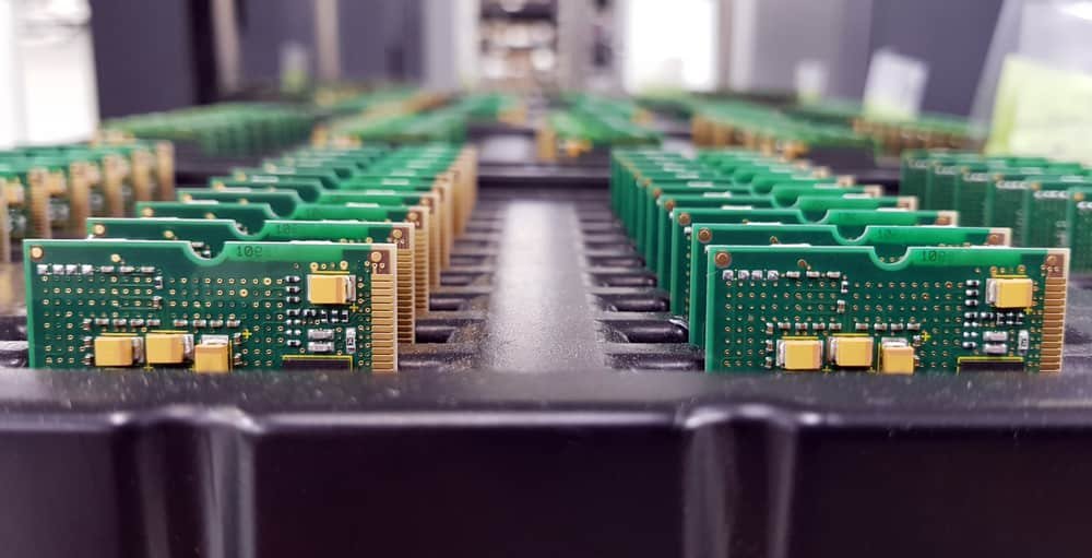
A board that cannot be tested ships on faith. The circuit may be entirely correct and the assembly may be flawless, and neither fact can be confirmed at the bench if the probes cannot physically reach the nodes that matter. Test access is decided during layout, and once copper is committed, adding it means a board revision.
Design for test planning settles the question while the board is still an editable file rather than a fabricated part. It costs very little at that early stage and grows more expensive at every stage afterward.
Why Test Access Gets Overlooked
Layout is a competition for space. Components must fit, high-speed routing must stay short, thermal relief must be provided, and mechanical constraints must be honored. Test points feel like a luxury against those demands, so they get deferred.
The consequence surfaces in the first article. A board fails, and the failing node sits under a ball grid array with no exposed access. Debug turns into guesswork. Sometimes an engineer scrapes a solder mask to reach a trace, which risks damaging the very unit under investigation. Planning access during prototype PCB manufacturing prevents that situation entirely.
Coverage Targets and Node Selection
Complete test coverage is rarely achievable, and pursuing it wastes board area. The useful target is coverage of nodes where failures are likely or consequential:
- Power rails and ground references, since supply problems produce symptoms that mimic logic failures
- Reset lines, clock nets, and configuration straps, which govern whether a device starts correctly
- Inputs and outputs of each functional block, allowing a technician to isolate a fault to a section rather than a whole board
Nets buried entirely under packages present the hardest cases. A via placed at layout to bring a signal to an accessible surface solves the problem when planned, and cannot be added afterward without a respin.
Physical Requirements for Probe Access
Test points must satisfy mechanical rules that vary by method. Flying probe systems require exposed metal of adequate size and clearance from neighboring features. In-circuit fixtures with spring-loaded pins impose stricter demands: consistent pad size, minimum spacing between adjacent points, and tolerance margin for fixture alignment.
Placement patterns matter as well. Test points concentrated on one side of the board simplify fixturing and reduce cost. Points clustered too tightly create mechanical interference between adjacent probes. Points too close to tall components block probe travel.
Choosing a Test Strategy Early
The test method influences layout, so the decision belongs at the design stage rather than after. Flying probe testing needs no custom fixture, which suits prototype and low-volume builds, though each unit takes longer to test. In-circuit testing runs quickly per unit and justifies its fixture cost at higher volumes. Functional testing exercises the assembly under operating conditions and depends on connector access and controllable inputs rather than probe points.
Most programs combine methods. Establishing the mix early lets PCB design services teams allocate the right access for each. Aerospace and defense customers frequently specify test point size, clearance, placement restrictions, and coverage percentages as formal deliverables, and meeting those specifications requires planning them into the layout from the beginning.
Verification Before Fabrication
Automated design for test analysis checks a layout against the chosen method, reporting inaccessible nets, undersized pads, spacing violations, and probes that would collide with components. Running this analysis before release turns test planning from an assumption into a verified result.
Partners providing PCB design services who perform the check as part of every layout catch problems that a designer focused on routing may miss. Pairing that verification with design for manufacturing analysis produces a board that fabricates cleanly, assembles reliably, and can be proven functional.
Carrying Coverage Into Production
Test access planned during prototyping keeps its value as volumes rise. The same points that supported bench debug support production fixtures, and the same coverage that isolated early faults isolates field returns. Programs treating prototype PCB manufacturing as the moment to establish testability avoid rebuilding that foundation later.
MJS Designs, Inc. is committed to providing the best in PCB design, assembly, and test engineering, with certified designers who apply design for test and design for manufacturing verification to every layout, plus flying probe and functional test capabilities in-house. With MJS Designs, you can trust that your board is testable from the prototype through full production.